Wednesday, September 29, 2010

Working on the bottom of the RF board

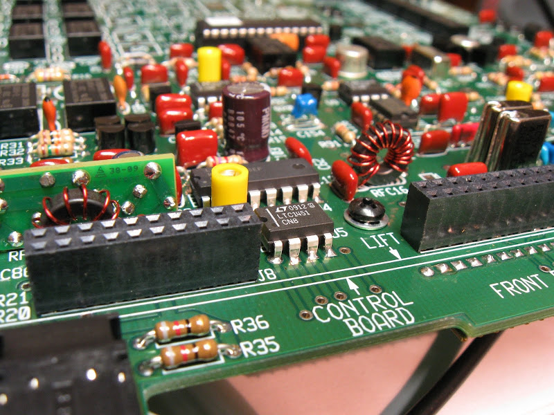
There are no pictures to post today, because there's not that much to see ... a modest number of parts distributed all across the bottom side of the RF board. It has turned out that installing parts on the bottom of the board has been the most difficult part of the project so far.

I found Elecraft's standard instruction to stuff some large number of components on bottom side of the board and then go and solder them all really didn't work for me. It almost seemed like I needed to customize in some fashion the installation of each component ... a bit of exaggeration, but I certainly did need to assess how I was going to install each component.

There were two main issues to deal with:

  1. Crowding on the top side of the board can make it necessary to solder a component on the bottom side of the board.
  2. You have to insure that no component is higher than the 2-D fasteners on the bottom of the board, so as to insure that nothing touches the bottom panel of the case when the K2 is assembled.

The instructions for installing components on the bottom board are prefaced with a brief paragraph that says basically "you may have to solder to the bottom of the board." In actuality, I soldered all the components in the last batch on page 59 on the bottom of the board, and I probably would have been better off soldering most of the components from the first batch on the bottom as well.

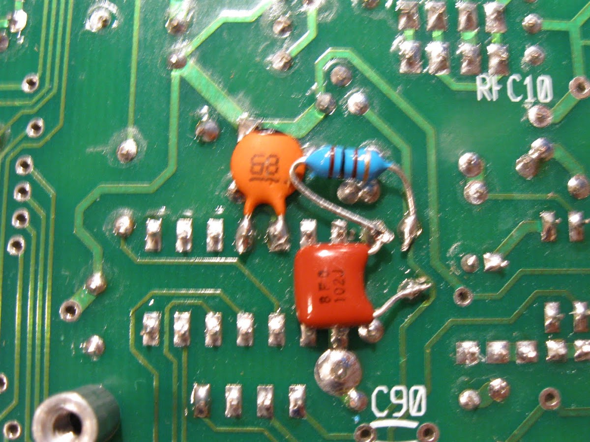
Soldering on the bottom was only really problematic for the monolithic capacitors, since they sit flush with the PC board and there is no lead exposed to solder to. For a lot of these, I ended up soldering them to the top of the board, even under some alarmingly crowded conditions. It turned out the solution was to put a 90° bend in the lead a very short distance away from the capacitor's body, trim the leads off, and then stuff them into their pads. The bend would expose the lead and then it was easy to solder. Depending on the size and location of the capacitor, it could then be bent upright or just left alone.

Thanks to Gary at Elecraft for helping me out with a couple of questions about bottom-side construction this week. In particular, he pointed out that C133's leads can be formed such that it sits lower than the nearby 2-D fastener and there is therefore no need to bend its body (which was a good thing, because there's really no place to bend it to!).

I took a day off from stuffing/soldering earlier in the week (I really needed a break!), and went ahead and wound L16 to L24 (on page 70). These will all now be waiting for me when I get to that stage of construction.

At the top of page 60 ...

Thursday, September 23, 2010

RF Board Top Front Completed

With L30 and L34, I stuffed the last two components on the front half of the top side of the RF board. The next step starts stuffing components starting in the left rear of the board, near the key jack.

I've wound six inductors so far, 3 RFCs and 3 transformers (one of which, T6, had a bifilar winding). Having figured out how to strip and tin the winding wire, I actually find winding the inductors to be very soothing. It's time-consuming, but the time passes very pleasantly and calmly.

Nearing the bottom of page 58 ...

Tuesday, September 21, 2010

First two RFCs

Today I started on the first of many RFCs and transformers to be wound on toroidal cores. This came with very specific instructions about how to strip the insulation off the enamel-coated wire. I practiced on a piece of scrap wire, but somehow couldn't manage to get the "blob on the tip of the soldering iron" method to work.

So, I took a look at the K2 forum, and found a variety of tips, none of which seemed like the answer to me, until I came across one response which referred to this awesome video (does require RealPlayer). Using an 800° tip on my Weller, the "scraping" step wasn't even necessary; I just held the tip of the iron there and stuffed solder in until ... voilà ... it "wet out" (to quote the guy in the video), and then I could just slide the tip and the solder down to the end of the lead. As the guy said, "solder is cheap" and I kept just stuffing it in there. Anyway, this worked like a charm; installing the RFCs, etc., has moved from the "scary" column to the "piece of cake" column.

By the way, the first RFC to be installed is RFC14, in that little space next to the thermistor daughter board. It was really no problem fitting it in; there again was "plenty" of room.

Monday, September 20, 2010

Grounding the crystals

Today was "install crystals on the RF board" day, including the scary instructions for double-grounding X7 to X11.

First, though, here's a picture of the current state of RF board construction. You can see X7 to X11 at the extreme right hand side of the picture.

After struggling to get the first ground wire on X7, I then went and checked the K2 forums to see what hints I could find. I wish I had looked there first! I used the following tips which various folks contributed to the forum, and it was pretty straightforward after that:

  • This was probably the most helpful hint (and non-intuitive, considering the dire warnings about overheating the crystals!!), namely to use an 800° tip, instead of the 700° tip I've been using.
  • I used some really fine grit sandpaper on the side of the crystal can (can't say it necessarily helped, but probably didn't hurt and may have helped).
  • I then applied a little solder to the side of the can.
  • I also had decided on my own to apply solder to each of the leads prior to installation.
  • Someone had a great hint about dropping the leads into the holes from the bottom of the board and soldering them to the board first. This was really the enabler for handling the inside leads (between the crystals and RP4).
  • I trimmed the leads in place to the correct length and used the "press it down with the flat end of a screwdriver" hint.
Anyway, there are all in, all grounded, and hopefully not overheated!

Next ... on to winding toroids!

Sunday, September 19, 2010

Middle of page 54

I've completed the section in which all the ICs are installed, along with some other odds and ends. The pile of un-installed components is noticeably smaller! Rather than post a "big picture" picture, I thought I'd post two detail shots.

Here's how the PLL stabilization modification to the RF board came out. This was apparently a design change made after the latest rev. of the RF board was frozen. It wasn't too hard to do; I must be getting more skilled at assembly!
Here's how it looks in the vicinity of that thermistor daughter board. It turned out the U6 (just to the left of the daughter board) fit in easily, and that there was still "plenty" of room to spare between the board and U6. So, I was able to bend the daughter board even more in the direction of U6, thus opening up more room to the right and actually putting a tiny bit more space between the thermistor board and C87.

Thursday, September 16, 2010

Lots of capacitors ...

Two fairly lengthy sessions and one shorter one resulted in my installing most of the front half of the RF board's diodes, transistors, and capacitors (all 68 of them!).

The instructions for stuffing the diodes and transistors emphasized the need to minimize lead length by getting the components as close to the board as possible. For all of these, I soldered one lead, then reheated it while pushing in the component, then soldered the remained leads.

With some practice, I'm getting better at forming the leads for the tiniest capacitors. They really need to be bent out at 90° from the body of the component, and then 90° again. The trick is to get the two "down" bends the correct distance apart; I'm getting better at it with practice.

I also installed the two components in the vicinity of the thermistor board that I was concerned about. Q19 was not a problem at all; it's very close to the thermistor board, but did not touch. Installing C87 did require, as the instructions suggested, bending the thermistor board slightly in the direction of U6. I was able to install C87, but its body just touches one of the soldered connections on the bottom of the thermistor board. That should not be a problem electrically, but I put a little piece of electrical tape between them anyway (visible in the photo). If I ever do this again, I'll really try to minimize the amount of solder I use on the thermistor board.

Tuesday, September 14, 2010

Lots of resistors and the thermistor board

I've completed installation of lots of resistors and a few resistor networks on the front half of the RF board. The last several steps of this were devoted to construction and installation of a small daughter board, first introduced in 2003 (as far as I can tell), which replaces RP3 and provides temperature compensation to the PLL, thus greatly reducing warm-up drift.

Here's the daughter board. It's quite small, occupying a space only slightly larger than an 8-pin resistor network. It in fact is installed on the motherboard in the same space as the original RP3. It was a bit tedious installing the 8 leads; I ended up doing the 90° bend first, then taping the lead down on the component side, and then soldering it in place.
Here's the thermistor board installed in the front left quadrant of the RF board.

It looks like getting C87 and RFC14 installed without shorting out to the back of the thermistor board will be difficult. Postings to the K2 forum all say "don't worry, it will all fit", but I think it may be necessary to put some electrical tape on the back of the thermistor board. It also looks like spacing for Q19 will be very tight. The instructions talk about checking to make sure that the thermistor board isn't shorting out to other components; this is not helpful at this point because the components haven't been installed yet!

For those keeping track ... just completed page 50.